Dead-Time Optimization in High-Frequency GaN Servo Drives: Third-Quadrant Conduction Loss, Bootstrap Clamping, and Torque Ripple Mitigation
Dead-time optimization for GaN servo drives: estimate reverse-conduction loss, assess bootstrap protection, and compare supplier evidence with an RFQ checklist.
Dead-time optimization in GaN servo drives means shortening reverse-conduction intervals while retaining a measured margin against cross-conduction. For engineers evaluating low-voltage servo inverters (24V–80V DC) at 50 kHz to 200 kHz PWM, that decision affects heat, bootstrap supply behavior, and current distortion. Higher switching frequency can reduce winding-current ripple and filter requirements, but does not by itself establish that a motor phase choke can be removed.
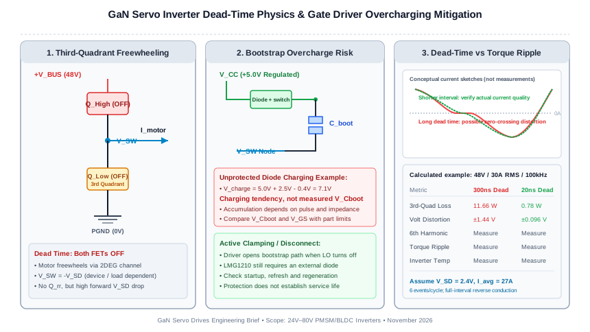
Unlike silicon MOSFETs, lateral enhancement-mode GaN transistors have no intrinsic p-n junction body diode. During dead time—when both half-bridge gates are commanded off—inductive current can flow through the GaN channel in the "third quadrant". The off-state reverse drop can be several volts; its value depends on the specific device, current, temperature, and gate bias. It must be taken from reverse-conduction curves or measurements, rather than treated as a fixed material constant.
Porting a 200 ns to 500 ns dead-time setting onto a 100 kHz GaN power stage can introduce avoidable reverse-conduction loss. Negative switch-node excursions can also overcharge an unprotected high-side bootstrap supply. Gate-voltage limits vary across GaN technologies: use the selected transistor and driver ratings, including any separately specified transient limits.
This technical guide analyzes the electrical physics of GaN dead-time optimization, derives the mathematical boundaries of third-quadrant conduction loss, examines bootstrap overcharge suppression mechanisms, and provides procurement and engineering teams with an actionable RFQ checklist to audit drive suppliers before hardware deployment.
Key Takeaways for Sourcing & Engineering Teams:
- Timing is device-specific: GaN has no body-diode reverse recovery, but output-capacitance commutation, propagation skew, and false turn-on still constrain dead time. A 20 ns setting is an example to qualify, not a universal safe value.
- Loss is calculable: Under the stated 30A RMS, 100 kHz assumptions below, reducing 350 ns to 20 ns changes estimated gross reverse-conduction loss from 13.61 W to 0.78 W.
- Bootstrap protection needs evidence: An active charging-path disconnect is one option. Verify floating-supply and gate-source voltages on the actual assembly.
- Torque improvement needs measurement: The simplified voltage-error model predicts a 93.3% reduction when moving from 300 ns to 20 ns. It cannot predict a noise reduction, torque-ripple percentage, or service life.
Published and reviewed: November 5, 2026. Scope: Global, English-language engineering and procurement guide for low-voltage (24V–80V DC) GaN brushless servo drives in robotics, cobots, AGV/AMR traction, and precision actuators. Calculations and diagrams are illustrative engineering models, not measured product results. This guide does not qualify medical equipment, functional safety, EMC compliance, or a supplier's current rating.
For a sourcing review, use the checklist below to prepare an OEM engineering inquiry with bus range, motor inductance, current, and cooling constraints.
1. The Physics of GaN Third-Quadrant Conduction
In silicon MOSFETs, off-state reverse current can flow through the intrinsic body diode. Its reverse-recovery charge contributes to turn-on current and loss when the complementary device commutates. Dead time primarily prevents overlapping channel conduction; lengthening it does not remove reverse recovery and can increase body-diode conduction.
The lateral enhancement-mode GaN HEMTs considered here use majority-carrier channel conduction rather than an intrinsic body diode. Zero body-diode Q_rr does not mean zero commutation energy: output capacitance, PCB parasitics, and any external diode still matter. Cascode and integrated-driver devices require their own datasheet interpretation.
1.1 Reverse Conduction Mechanism
When a GaN FET is turned off by bringing its gate-to-source voltage below its threshold (V_GS < V_th), it can still conduct current in reverse, from source to drain.
As reverse current is forced into the source terminal by the inductive motor winding, the drain potential drops below the source potential. When the drain voltage drops low enough such that the gate-to-drain voltage exceeds the threshold voltage:
V_GD = V_G - V_D > V_th
The channel starts to conduct in reverse. Since V_GD = V_GS,off + V_SD, the approximate onset condition is:
V_SD,onset ≈ V_th - V_GS,off
Where:
V_this the device's threshold under its specified measurement conditions.V_GS,offis the applied off-state gate bias.- At finite current, extra channel overdrive and resistance increase the drop. Use the manufacturer's reverse I–V curves at the relevant bias and junction temperature; the onset equation is not a complete loss model.
1.2 The Negative Gate Bias Dilemma
Negative gate bias can improve immunity to Miller-current-induced false turn-on, but also increases the reverse-conduction onset voltage. With an illustrative V_th = 1.5V and V_GS,off = -2.5V:
V_SD,onset ≈ 1.5V - (-2.5V) = 4.0V
This 4.0V figure is an onset estimate, not the loaded drop at 30A. For devices specified for 0V turn-off, a low-impedance pull-down and compact gate loop can avoid the extra reverse-drop penalty of negative bias. Check allowable negative gate voltage and measured ringing before selecting a drive scheme; no single gate-loop inductance guarantees immunity.
2. Quantifying Dead-Time Power Loss in a 3-Phase Servo Inverter
For continuous, center-aligned PWM with each half-bridge switching twice per carrier cycle, there are two dead-time intervals per phase per period. This covers the assumed SPWM or continuous SVPWM example; discontinuous PWM, pulse suppression, and clamped legs change the event count.
Across all three phases, there are six dead-time conduction events per PWM cycle.
2.1 The Mathematical Loss Model
An approximate gross reverse-conduction loss across a balanced three-phase inverter is:
P_dead_total = 6 × f_sw × t_dead × V_SD × I_phase,avg
This estimate assumes current commutates immediately into off-state reverse conduction for the entire dead interval, with a constant assumed V_SD. Output-capacitance charging can occupy part of that interval, especially near zero current. It excludes channel conduction outside dead time, switching energy, gate-drive power, and controller losses; the result is not total inverter loss or a guaranteed net saving.
Where:
f_swis the inverter switching frequency (e.g., 100 kHz).t_deadis the inserted dead time (e.g., 20 ns vs 300 ns).V_SDis the third-quadrant reverse drop (assumed to be 2.4V in this example).I_phase,avgis the average rectified phase current during commutation (≈ (2 / π) × I_peak = (2√2 / π) × I_RMS ≈ 0.90 × I_RMS).
2.2 Numerical Scenario: 48V DC Bus, 30A RMS Motor Current, 100 kHz PWM
Consider an illustrative design scenario, not a tested product, operating at:
- DC bus:
V_BUS = 48V - Phase current:
I_RMS = 30A(I_phase,avg ≈ 27A) - Switching frequency:
f_sw = 100 kHz(T_PWM = 10 µs) - GaN
V_SD = 2.4V
Using the rounded I_phase,avg = 27A, compare three candidate settings:
- Long baseline setting on the same GaN stage (
t_dead = 350 ns):
P_dead = 6 × (100 × 10³) × (350 × 10⁻⁹) × 2.4 × 27 = 13.61 Watts - Intermediate Conservative Setting (
t_dead = 100 ns):
P_dead = 6 × (100 × 10³) × (100 × 10⁻⁹) × 2.4 × 27 = 3.89 Watts - Short candidate setting, requiring qualification (
t_dead = 20 ns):
P_dead = 6 × (100 × 10³) × (20 × 10⁻⁹) × 2.4 × 27 = 0.78 Watts
+-----------------------------------------------------------------------------------+
|               3-Phase Inverter Dead-Time Power Dissipation (100kHz, 30A RMS)      |
+-----------------------------------------------------------------------------------+
|  350 ns (GaN Baseline)   | ============================================= 13.61 W  |
|  100 ns (Conservative)   | ============= 3.89 W                                   |
|   20 ns (GaN Candidate)  | == 0.78 W                                              |
+-----------------------------------------------------------------------------------+
The estimated difference is 12.83 W before other loss terms are considered. Converting that into junction temperature requires a validated thermal impedance, housing interface, ambient temperature, and duty cycle. At locked rotor, phase currents are not the balanced time-varying sinusoids assumed here; sum the actual phase-current magnitudes and switching events instead of automatically using 0.90 × I_RMS.
For compact joint actuator integration, review our hardware architectures on the robot joint servo drive overview and 10A micro robot joint solution.
3. The Bootstrap Overcharging Danger Under Negative Switch-Node Undershoot
Alongside conduction loss, review the interaction between third-quadrant conduction and the high-side bootstrap supply circuit.
3.1 The Undershoot Mechanism
In a bootstrap-powered half-bridge, a capacitor (C_boot) supplies the floating high-side driver. When the low-side switch (Q_Low) is on, the switch node (V_SW) is approximately at ground. For an illustrative 5V rail, charging through a diode gives:
V_Cboot = V_CC - V_diode ≈ 5.0V - 0.5V = 4.5V
During an interval with positive phase current flowing from the inverter into the motor, current can freewheel from ground through the off-state low-side device. The switch node is then pulled negative by the reverse drop:
V_SW ≈ -V_SD; for the following charging example, assume V_SD = 2.5V.
Parasitic loop inductance (L_loop × di/dt) can add a deeper transient. Its magnitude and duration must be measured with suitable high-bandwidth differential probing at the device terminals.
3.2 Gate-Supply Stress and Device Limits
For an unprotected diode-fed bootstrap, the simplified charging-loop voltage during a sustained negative excursion is:
V_Cboot,effective = V_CC - (-V_SD) - V_diode = 5.0V + 2.5V - 0.4V = 7.1V
The 7.1V result is a charging tendency, not proof that the capacitor reaches 7.1V during one short pulse. Actual accumulation depends on charging impedance, capacitance, pulse duration, repetition, and driver consumption. A floating-supply measurement is also distinct from the actual high-side gate-to-source waveform.
Gate structures and ratings differ across manufacturers. Compare both measured waveforms against the selected parts' recommended operating ranges and absolute maxima; a 6V example must not become a universal GaN limit. Repetitive overstress can degrade or damage a gate, but this arithmetic does not establish a failure time or mechanism.
3.3 Gate Driver Solutions for Bootstrap Protection
Three options to assess for bootstrap overcharge protection are:
- Active bootstrap-path disconnect: The TI LMG1210 product documentation describes an internal switch that disables charging through an external bootstrap diode when the low-side output is off. It does not replace that diode. Validate startup, refresh, and negative switch-node behavior in the actual circuit.
- Dedicated Bootstrap Zener or Shunt Clamping: A suitably designed shunt across the floating supply can limit overcharge. Select it using its dynamic clamp voltage, tolerance, pulse energy, leakage, and layout. A nominal 5.1V Zener does not guarantee a 5.2V ceiling, and repetitive clamping has a thermal cost.
- Isolated DC-DC Gate Power Supplies: A regulated bias supply referenced to each high-side source removes dependence on bootstrap refresh. Continuous high-side operation still requires a driver and logic interface that support it, adequate isolation/CMTI, and acceptable supply ripple. It adds parts and parasitic coupling; isolation alone does not establish reliability.
4. Phase-Current Distortion and Torque Ripple at Zero Crossings
In motion control applications, dead time is not merely a power stage efficiency concern; it directly impacts servo control accuracy, torque smoothness, and acoustic emissions.
4.1 The Voltage Error Vector
During dead time, neither switch in a half-bridge is actively commanded on. Once capacitance commutation is complete, the approximate switch-node clamp depends on phase-current polarity:
- When phase current flows into the motor (
I_phase > 0), current freewheels through the low-side switch in third quadrant, pullingV_SWto-V_SD(effectively ground). - When phase current flows out of the motor (
I_phase < 0), current freewheels through the high-side switch, pullingV_SWtoV_BUS + V_SD(effectively the DC rail).
The resulting simplified average pole-voltage error (ΔV) over each PWM period is:
ΔV = -sign(I_phase) × V_BUS × (t_dead / T_PWM)
This simplified average pole-voltage model neglects reverse drop, capacitance transitions, and delay asymmetry. Motor phase-to-neutral error also depends on common-mode subtraction. Close to zero current, ripple and uncertain polarity make the sign approximation less reliable.
4.2 Impact on Low-Inductance Motors
For a low-inductance motor, a given voltage error produces a larger current-slope error (di/dt = ΔV / L). The relevant incremental inductance depends on rotor position, current, and measurement frequency; obtain motor data rather than inferring inductance from construction alone.
In these motors:
- A 350 ns dead-time setting at 100 kHz PWM represents a 3.5% duty-equivalent error (
350 ns / 10 µs) in this model. - Around current zero crossings, dead-time nonlinearity can create a "flat spot" (zero-current clamping distortion) in the phase-current waveform.
- Current harmonics associated with dead-time distortion can appear as sixth-order components in the rotating FOC frame. Their torque contribution depends on the motor and control loop.
- Current distortion can contribute to vibration and audible noise, alongside cogging, PWM excitation, mechanics, and current-sensor errors.
At 48V and 100 kHz, the model gives |ΔV| = 1.44V at 300 ns and 0.096V at 20 ns: a 93.3% reduction in this modeled error term. It does not imply a 93.3% torque-ripple reduction or a specified acoustic improvement. Compare synchronized phase-current, torque, and acoustic measurements at identical speed, load, current-loop settings, and temperature. Compensation may still be needed for residual delays and current-polarity uncertainty.
5. Architectural Comparison: Dead-Time Management Strategies
This matrix compares design decisions and the evidence needed to select them. It does not rank suppliers or assign efficiency figures to entire device families.
| Decision | Discrete GaN with diode-fed bootstrap | GaN with charging-path disconnect | Integrated GaN power stage | Evidence required |
|---|---|---|---|---|
| Dead-time setting | Controller and driver delays both matter | Driver may provide local adjustment | Internal timing may be fixed or configurable | Both edges measured over voltage, load, and temperature |
| Reverse-conduction loss | Depends on FET bias and reverse I–V | Shorter qualified intervals can reduce loss | Integration does not remove channel reverse drop | Device curves plus actual switching-event count |
| Bootstrap overcharge | Negative switch-node voltage can add charge | Disconnect reduces this charging path | Protection varies by part | Floating-supply and gate-source waveforms |
| CMTI and false turn-on | Depends on driver, layout, and gate impedance | Bootstrap protection does not prove CMTI | Internal layout helps reduce external gate-loop exposure | Datasheet conditions and assembly transient tests |
| Continuous high-side duty | Requires refresh or auxiliary bias | Disconnect alone does not enable DC operation | Check refresh or charge-pump provisions | Maximum on-time and minimum refresh interval |
| Current and thermal capacity | Set by FETs, PCB, and cooling | Driver choice does not establish phase-current rating | Package thermal path may dominate | Continuous/peak phase current, duration, and ambient |
| Torque quality | Timing and compensation both matter | Local timing can reduce one error source | Integration is not a torque specification | Current FFT and torque data on the intended motor |
| Lifecycle and serviceability | More independently sourced components | Specific driver availability matters | More functions depend on one device family | Lifecycle status, change notices, and requalification plan |
To compare standard discrete boards versus micromodules, explore our monolithic GaN micromodules guide and the catalog of GaN low-voltage servo drives.
6. Engineering Tuning: Setting Dead Time Without Shoot-Through
Qualifying a short dead time requires analyzing the complete command-to-channel path in both directions. The following 20 ns budget is an illustrative screening example; its numbers are assumptions, not guaranteed LMG1210 limits.
Illustrative command dead-time budget:
8 ns assumed worst-path skew + 4 ns channel release + 8 ns margin = 20 ns
Replace every input with guaranteed limits and assembly measurements.
6.1 A Command-to-Channel Timing Budget
A screening inequality for one commutation direction is:
t_dead,cmd >= (t_p,off,max + t_release,max) - (t_p,on,min + t_conduct,min) + t_margin
Where:
t_p,offandt_p,oninclude propagation through the controller output, isolator or level shifter, and driver. Use compatible timing definitions and worst-case conditions. A typical channel-matching number is not a worst-case guarantee.t_releaseandt_conductdescribe channel turn-off and turn-on after the corresponding driver output transition. Drain-voltage fall time alone does not establish when the channel stops conducting.t_margincovers remaining uncertainty in measurement, jitter, temperature, supply, layout, and component variation. Recalculate for the opposite edge; asymmetric hardware may need different settings.
Illustrative screening result:
t_dead,cmd ≈ 8 ns (assumed skew) + 4 ns (release) + 8 ns (margin) = 20 ns, conservatively omitting incoming turn-on latency.
Non-overlap is only one constraint. Available load current must also commutate output charge; a rough transition estimate is t_comm ≈ Q_comm / |I_phase|, with voltage-dependent charge from both devices. Near zero current, a transition may remain incomplete despite non-overlapping gates. Validate switching energy, bus-current spikes, ringing, and device temperature rather than shortening dead time solely to meet a nominal number.
6.2 Resistor-Programmable Hardware Dead Time vs DSP Software Generation
Engineering teams face a choice between generating dead time in the digital controller (DSP or FPGA) or using driver hardware pins:
- DSP or MCU PWM Generation (Independent Input Mode): Verify the selected timer's edge resolution, clock tolerance, and update behavior. Digital isolators and level shifters add delay and skew. Fine timer resolution does not prove equally accurate gate timing, and independent driver inputs may require external interlocking.
- Hardware-Set Driver Dead Time (e.g., LMG1210 PWM Mode): TI specifies a single-input PWM mode with independently adjustable edge dead times from 0 to 20 ns, as well as an independent-input mode. Local complementary generation reduces dependence on separate upstream paths. It is not a functional-safety guarantee or proof of correct behavior during every controller fault.
Before accepting a supplier's timing claim, ask for probe locations, deskew method, bandwidth, and operating conditions. Test startup, motoring, regeneration, low current, and fault shutdown. Agree on device-specific voltage limits and acceptable temperature rise before comparing candidate settings.
7. Procurement and Engineering RFQ Sourcing Checklist
When sourcing GaN servo drives, compare documented behavior under matching conditions. A GaN label or short nominal dead time does not establish application suitability.
Include the following mandatory requirements in your Request for Quote (RFQ) and engineering qualification matrix:
- 1. Timing definition and range: Request commanded and measured effective dead times for both edges, including PWM mode, resolution, jitter, and worst-case conditions. Ask why the setting was selected; do not reject a design solely for exceeding an arbitrary nanosecond threshold.
- 2. Device and driver identification: Request exact part numbers, revisions, gate-bias requirements, control mode, and the actual bootstrap protection schematic. Confirm the chosen variant's functions rather than assuming every member of a driver family includes a clamp.
- 3. Bootstrap and gate-voltage evidence: Request
V_HB - V_HSand high-sideV_GScaptures during startup, maximum permitted duty, regeneration, and current reversal. Compare against device-specific operating and transient limits, including probe uncertainty. - 4. Gate-rail tolerance: Review regulation, startup overshoot, ripple, and temperature drift over the input supply range. Agree on tolerances from the transistor and driver requirements rather than prescribing one regulator type or a universal 5V rail.
- 5. Layout and transient evidence: Request gate/power-loop layout, inductance extraction method if available, and measured ringing at the device pins. A small extracted inductance is useful context but not an independent acceptance criterion.
- 6. Thermal and current qualification: Require continuous and peak phase-current definitions, peak duration, ambient, cooling interface, PWM frequency, and a recorded duty profile. Include controlled low-speed or locked-rotor tests within component and motor limits; a hot spot alone cannot identify the loss mechanism.
- 7. Motor-control quality: Request phase-current FFT and torque-ripple data on the intended motor or a justified equivalent, with inductance, speed, load, sensor bandwidth, and controller settings. Separate predicted voltage-error reduction from measured torque and noise.
- 8. Fault behavior and release records: Ask for reset, missing PWM, undervoltage, overcurrent, and shutdown behavior, including any independent interlock. Record firmware/hardware revisions and test coverage; dead-time control alone does not establish STO or another safety function.
Use this completed checklist when discussing GaN low-voltage servo drive requirements. Keep unverified fields marked unknown and make the required evidence part of sample acceptance before volume purchasing.
8. Frequently Asked Questions
Why is dead time so much more critical in GaN inverters than in Silicon MOSFET inverters?
Off-state GaN reverse conduction can have a higher drop than a silicon body diode, making long intervals costly at high PWM frequency. Instantaneous conduction power is P = |I| × V_SD; energy per interval is approximately E = |I| × V_SD × t_dead. Multiplying by the event rate gives average power. Actual device curves and timing are needed for a quantitative comparison.
Can an anti-parallel Schottky diode be placed across each GaN FET to reduce third-quadrant loss?
Sometimes. A suitably placed diode can share reverse current, but loop inductance can delay its conduction and junction capacitance adds switching energy. Compare the diode's measured current, capacitance loss, temperature, and cost over the intended operating range. Neither universal benefit nor universal rejection follows from a nominal 20 ns interval.
What causes bootstrap capacitor overcharging in a GaN half-bridge?
Negative switch-node voltage increases the charging-loop voltage of a diode-fed bootstrap. Repeated pulses may accumulate excess charge depending on circuit impedance and discharge. Measure the floating supply and gate-source voltage, then assess them against the selected parts' limits. An active disconnect or properly qualified clamp can address the charging path.
How does dead-time optimization affect acoustic noise in robot joints?
Reducing dead time can reduce one source of current distortion and related vibration. The example's 93.3% voltage-error reduction is not a sound-pressure prediction. Validate with the same motor, mechanical assembly, speed, load, microphone position, and control settings; mechanical resonances and other electrical harmonics may dominate.
What is the trade-off of reducing dead time below 10 ns?
There is no universal 10 ns boundary. Shortening below the actual non-overlap requirement risks cross-conduction. Shortening below the available output-charge commutation time can also increase hard-switching loss without causing overlap. Evaluate both effects over current, voltage, temperature, and both edge directions; low-current behavior can set a different optimum from rated-load behavior.
Does adaptive dead time eliminate the need for hardware margins?
No. Adaptive implementations vary: sensing delay, noise immunity, minimum/maximum timing, current reversal, startup, and fault fallback all matter. Compare their qualified operating envelope with a fixed-setting design. A fixed 20 ns setting is not inherently safer or more accurate without equivalent evidence.
9. Next Steps for Engineering and Sourcing
Select a dead-time strategy from a documented loss model, measured timing margin, bootstrap/gate-voltage records, and motor-control tests. The calculations here help prioritize questions and compare evidence; they do not certify inverter efficiency, acoustic performance, or operating lifetime.
- To discuss candidate hardware and the evidence required for your operating point, review our GaN low-voltage servo drive family and EtherCAT 48V servo drive modules.
- For battery-powered warehouse robotics, compare the integration requirements for AMR and mobile robot servo drives, including peak-current duration and high-side refresh constraints.
- If your program requires custom form-factor actuator integration, circular hollow-shaft boards, or direct thermal interface modeling, initiate an OEM custom engineering discussion with our motion control hardware team.
Sources and References
Manufacturer references below provide component and design context. The TI product page and Infineon technology hub were checked November 5, 2026; the two TI application-note titles and destinations were matched to the product page's documentation index, without separately opening the PDFs. Worked examples and waveform sketches in this article are illustrative, not manufacturer or first-party hardware benchmarks.
-
Texas Instruments — LMG1210 product information and datasheet index. Primary source for the external bootstrap diode with internal disconnect switch, single-input PWM and independent-input modes, and adjustable edge dead times. Component features do not establish a complete servo drive's performance.
-
Texas Instruments — Implementing Bootstrap Overcharge Prevention in GaN Half-bridge Circuits, SNVAA94. Application-note reference listed by TI for further bootstrap protection design review; consult the full document and selected device datasheets before implementation.
-
Texas Instruments — Optimizing efficiency through dead time control with the LMG1210 GaN driver, SNVA815, Rev. A. TI-listed further reading on dead-time control. The article's 48V/30A calculations are independent assumed scenarios, not results attributed to this note.
-
Infineon Technologies — Gallium nitride technology and product overview. General technology and product-family context. This is a product hub, not a white paper or evidence for a particular torque harmonic, voltage rating, or efficiency figure.
Author

More Posts
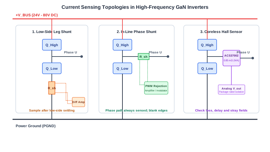
Current Sensing Architectures in High-Speed GaN Servo Drives: In-Line Phase Current vs Low-Side Shunts vs Coreless Magnetic Sensors
Compare current sensing in GaN servo drives: low-side shunts, in-line shunts and magnetic sensors. Use timing and thermal examples plus an RFQ checklist to select.

Dual Absolute Encoder Integration in High-Speed GaN Servo Drives: BiSS-C & SSI Signal Integrity, Dual-Loop FOC Latency, and Mechanical Compliance
Dual absolute encoder integration in GaN servo drives: compare BiSS-C and SSI, budget feedback delay, and use an RFQ checklist to qualify your drive supplier.
GaN vs Silicon MOSFETs in Low-Voltage Servo Drives: Thermal & Power Density Compared