
Short-Circuit Withstand Time and Ultra-Fast Fault Protection in GaN Servo Drives: Nanosecond Desaturation, Two-Stage Soft Turn-Off, and Inverter Sourcing
Compare short-circuit protection in GaN servo drives: evaluate detection timing, soft turn-off, and fault coverage. Use the RFQ checklist to screen suppliers.
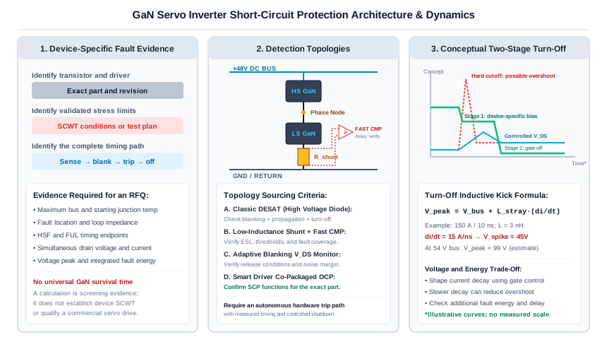
Short-circuit protection in GaN servo drives must be selected for the actual transistor, fault path, bus voltage, and starting junction temperature. There is no universal GaN short-circuit withstand time (SCWT), nor a universal sub-100 ns clearance requirement. The useful purchasing question is whether the complete hardware protection path clears each specified fault within the selected device's validated stress limits, while controlling turn-off overvoltage.
A pinched AGV motor cable and shoot-through inside an integrated robot joint can impose very different fault currents and inductances. A fast comparator specification alone cannot establish protection: sensing, blanking, propagation, gate discharge, and current decay all contribute to the stress experienced by the switch.
This guide compares six sensing architectures, explains nanosecond desaturation and two-stage soft turn-off, and provides an eight-point RFQ checklist. Use it to compare supplier evidence before selecting an inverter.
Key sourcing and engineering takeaways:
- Specify the device and conditions. Require the exact GaN part number, bus limits, initial junction temperature, and fault-loop impedance behind any SCWT claim. An unspecified rating is an open qualification item.
- Compare complete timing paths. Detection latency, PWM-to-gate propagation, and fault-current clearance are different measurements. Firmware notification should follow an autonomous hardware shutdown where the device requires fast protection.
- Control voltage and energy together. Slower turn-off can reduce
L · di/dtovershoot but increases the time the switch dissipates fault energy. Validate both limits on the actual board. - Do not assume integrated protection. An integrated gate driver or undervoltage lockout does not establish short-circuit protection. Read the functions and limits for the exact device revision.
- Request HSF and FUL evidence. Waveforms need defined timing markers, probe setup, temperature, fault impedance, and a documented post-test result.
Published and reviewed: November 11, 2026. Scope: Global, English-language engineering selection guide. The intended application is nominal 24 V to 60 V DC battery-powered servo systems, including mobile robots and integrated joints. Current capability, cooling, grounding, and allowable transients remain product-specific. High-voltage sources below illustrate protection principles; their ratings must not be transferred to low-voltage devices.
Method and limitations: This is a source-based engineering review with explicitly hypothetical electrical calculations, not a report of our own destructive testing. It does not certify any drive's fault survival, functional safety, or repetitive fault endurance. Device-specific transient models and qualified laboratory evidence are required to turn a screening calculation into an acceptance limit.
For an initial shortlist, compare the GaN low-voltage servo drive series, the 48V servo driver board, and the 100A robot joint servo drive. Ask for the same fault evidence for every candidate; these links do not imply that a model has passed the tests described here.
1. The Physics of GaN Short-Circuit Vulnerability
1.1 Channel Stress and Instantaneous Power
Enhancement-mode GaN HEMTs conduct through a two-dimensional electron gas at a semiconductor heterojunction. Low on-resistance and fast switching are useful in a compact inverter, but neither property specifies the energy a transistor can withstand during a short circuit. Gate structure, die geometry, package, gate bias, and operating temperature all affect the result.
During a fault, substantial drain voltage can coincide with high drain current. Consider a hypothetical switch carrying 180 A while sustaining 48 V:
P_fault = V_DS × I_D = 48 V × 180 A = 8.64 kW
E_SC = ∫ V_DS(t) · I_D(t) dt
E_SC,example = 8640 W × 250 ns = 2.16 mJ
The energy calculation assumes constant voltage and current throughout the interval. A real waveform requires integration of simultaneous voltage and current measurements, with probe delay corrected. The example establishes electrical energy only; it does not prove that a particular device survives 250 ns.
1.2 Why a Thermal Estimate Cannot Establish SCWT
A small thermal mass can heat quickly, but a single bulk heat-capacity estimate cannot determine the local peak channel temperature during a sub-microsecond event. Heat spreads within the semiconductor even when little has reached the external heatsink. Effective heated volume, nonuniform current distribution, temperature-dependent behavior, and electrical breakdown mechanisms matter.
Consequently, do not derive a universal failure temperature or survival window from an assumed active-layer volume. Obtain the manufacturer's specified short-circuit capability, if available, and its test conditions. If no SCWT is guaranteed, record that limitation and agree on an application qualification plan rather than converting typical switching specifications into a survival rating.
Distinguish intrinsic withstand time from protected fault response. A published shutdown time describes a particular circuit and measurement endpoint; it does not establish the unprotected die's destruction time. Production acceptance should compare the complete measured stress with agreed device limits, including tolerances and margin.
2. Fault Typology: Hard-Switching Fault vs Fault-Under-Load
2.1 Hard-Switching Fault (HSF)
An HSF occurs when a transistor turns on into an existing short. Depending on the conducting switches and return path, the current may be limited mainly by local bus impedance, semiconductor behavior, or motor wiring. The device voltage may fail to fall to its expected on-state value, making drain-voltage monitoring useful after an appropriate turn-on blanking interval.
A short across motor terminals is not automatically equivalent to directly shorting a transistor across the DC link. Document the inverter switching state and fault fixture. Otherwise, two suppliers can both label their captures “HSF” while applying different stresses. Shoot-through in one half-bridge also deserves explicit coverage because its loop can bypass much of the motor cable inductance.
2.2 Fault-Under-Load (FUL)
In an FUL event, the inverter is already carrying load current when the fault appears. Initial current rise can be screened with:
di/dt ≈ V_loop / L_loop
Example: 48 V / 150 nH = 320 A/µs = 0.32 A/ns
This assumes the stated voltage is applied across the fault-loop inductance and neglects resistance and semiconductor voltage drops. It is not a prediction for every motor terminal fault. The current threshold may be crossed before drain voltage rises enough to trigger a desaturation detector, so sensing architecture affects which event becomes visible first.
For both HSF and FUL, require an explicit start marker and end marker. Current crossing a threshold, fault-pin assertion, gate voltage falling, and current reaching a safe residual level are distinct events. Define which interval a quoted “response time” actually measures.
3. Nanosecond Desaturation: Blanking and False-Trip Trade-Offs
3.1 The Blanking Time Dilemma
Conventional DESAT monitors switch voltage through a sensing network and masks the normal turn-on transition. A simplified capacitor-charging relationship is:
t_blank ≈ C_blank · V_threshold / I_chargeThis expression excludes internal driver delays, initial capacitor voltage, clamps, and filter behavior. A circuit designed around a microsecond-scale blanking interval cannot be assumed to protect a device with a shorter validated stress window. Conversely, reducing the capacitor does not establish a complete nanosecond protection path.
For a schematic review, request maximum blanking and propagation delays across temperature and supply tolerance. Then include the turn-off trajectory. A supplier should explain why its noise rejection does not conceal the fault and why its fastest shutdown does not create an excessive voltage peak.
3.2 Capacitive Displacement and False Trips
Capacitance in a high-voltage sensing diode or PCB coupling path injects displacement current during a switching edge. For an illustrative coupling capacitance and slew rate:
I_disp = C_coupled · dV/dt = 2 pF × 50 V/ns = 100 mAThat pulse can disturb a sensitive input, but actual false-trip behavior depends on pulse duration, clamps, impedance, polarity, and filtering. The 50 V/ns assumption is a calculation input, not a minimum servo-drive requirement. Request immunity evidence at the candidate's specified switching slew rates and operating points.
An adaptive blanking scheme may use gate state or switch-node behavior to shorten masking. Its sensing threshold and release condition must be checked against the actual GaN device. Threshold voltage and a gate-charge plateau are different quantities; neither defines a universally safe intermediate gate bias.
4. Architecture Comparison: Six Fault-Detection Topologies
Table 1 compares design trade-offs rather than assigning unsupported typical timing ranges. No row establishes complete inverter protection without application evidence. Shunt losses are calculated examples at 50 A RMS, using P = I²R; they exclude comparator supply consumption and other inverter losses.
| Sensing architecture | Timing evidence to request | Switching-noise concern | Added power-path loss | Integration trade-off | Procurement decision |
|---|---|---|---|---|---|
| Classic diode DESAT | Maximum blanking, filter, comparator, and shutdown delays | Diode capacitance and switch-node coupling | No series shunt loss | Familiar circuit; timing may be unsuitable | Accept only with a demonstrated device-specific stress margin |
| Low-side shunt with filtered amplifier | Amplifier settling and hardware trip delay, including filters | Common-mode recovery and ground bounce | 2.5 W at 1 mΩ | Can share control sensing, but filtering adds delay | Do not treat an ADC measurement path as automatic SCP |
| Low-inductance Kelvin shunt with fast comparator | Threshold-to-output delay and complete current-clearance waveform | Shunt ESL, routing pickup, input overdrive | 1.25–3.75 W at 0.5–1.5 mΩ | Direct signal; heat and routing require review | Verify coverage for every switching state and fault path |
| Adaptive-blanking V_DS monitor | Worst-case release time, threshold tolerance, and fault response | Normal turn-on ringing versus genuine desaturation | No series shunt loss | Device- and layout-dependent calibration | Require HSF and FUL captures across conditions |
| Integrated protected GaN stage | Exact OCP/SCP functions, threshold limits, and timing definitions | Internal sensing helps, but board parasitics remain | Device-specific; no external shunt necessarily required | Compact integration; functions vary by part | Confirm SCP explicitly; driver integration alone is insufficient |
| Rogowski or PCB inductive sensing | Integrator bandwidth, reset behavior, and complete trip delay | Magnetic cross-talk and switching pickup | No resistive series sensing loss | Measures changing current; needs signal reconstruction | Combine with suitable sustained-current monitoring where needed |
4.1 Low-Inductance Shunt and Comparator
A shunt plus hardware comparator offers a directly inspectable signal path. Its parasitic inductance can also produce a voltage unrelated to the resistive current signal. For assumed values:
V_error = L_ESL · di/dt = 1 nH × 5 A/ns = 5 V
V_shunt = 150 A × 1 mΩ = 150 mV
Kelvin connections and appropriate shunt geometry reduce sensing errors but do not remove every parasitic contribution. Check input protection, comparator common-mode range, threshold tolerance, and measured recovery after switching edges. Placement in the DC return or individual legs determines which fault currents are observable. See the related current sensing architecture guide when preparing the sensing portion of an RFQ.
4.2 Adaptive Blanking and Active V_DS Monitoring
Adaptive monitoring trades fixed masking time for additional circuit complexity. Ask what releases the blanking interval, what happens if the monitored edge is abnormal, and how component tolerances affect fault detection. Low on-state voltage can make accurate thresholds difficult; a higher threshold may detect only after the switch has entered a more stressful condition.
Do not accept a nominal comparator delay as evidence for the entire sensing network. Require the supplier to identify the worst covered fault and any state in which sensing is disabled. A parallel fast current path can improve coverage, but its added complexity also needs verification.
4.3 Integrated Driver Does Not Mean Integrated SCP
The TI LMG2100R044 product documentation describes a low-voltage GaN half-bridge with integrated driver, bootstrap clamping, and supply undervoltage lockout. Those functions alone do not establish a complete short-circuit protection claim. Check its datasheet and the surrounding inverter circuit rather than inferring SCP from the word “protection.”
For a contrasting example, TI's LMG352xR030 datasheet, section 5.6, specifies short-circuit turn-off times using defined current endpoints. It lists 65 ns typical and 100 ns maximum for an already-on device under the stated ramp conditions, versus 80 ns typical and 180 ns maximum when turning on into a short. This is a 650 V device family, cited to demonstrate timing definitions, not to specify a 48 V servo inverter. Section 7.3.7.1 distinguishes cycle-by-cycle OCP from latched SCP.
For a relevant low-voltage architecture reference, TI's TIDA-010936 design uses LMG2100 half-bridges in a 12 V to 60 V motor-drive power stage. Its application relevance does not establish qualification of another manufacturer's drive.
Before requesting samples, review OEM customization options and ask suppliers to identify their exact sensing and shutdown paths against Table 1.
5. The Inductive Turn-Off Paradox and Two-Stage Soft Turn-Off
5.1 The Stray-Inductance Voltage Spike
Abrupt current interruption can produce voltage overshoot. Consider a hypothetical 150 A current reduction in 10 ns through 3 nH of effective commutation inductance:
|di/dt| = 150 A / 10 ns = 15 A/ns
V_spike ≈ L_stray · |di/dt| = 3 nH × 15 A/ns = 45 V
V_DS,peak ≈ 54 V + 45 V = 99 V
The 54 V bus is an assumed transient operating point, not a universal maximum for nominal 48 V batteries. This simple estimate omits capacitance, clamp paths, resistance, and ringing. Nevertheless, it identifies a voltage-budget concern for an 80 V switch. A nominal 100 V rating would also leave little headroom in this example; use the actual continuous and transient ratings.
Do not equate lack of an avalanche-energy specification with proof that every excursion above a nominal voltage instantly destroys every GaN device. EPC's manufacturer support guidance points to device-specific overvoltage ratings. For procurement, the practical rule is to stay within documented limits and avoid assuming silicon-style avalanche absorption where none is specified.
5.2 Mechanics and Limits of Two-Stage Soft Turn-Off
Two-Stage Soft Turn-Off can shape gate discharge to moderate fault-current decay before final turn-off. A conceptual sequence is:
Hardware fault detected and latched
  -> controlled gate discharge / intermediate gate bias
  -> current decay with V_DS and energy monitored during qualification
  -> final gate-off state specified by the device manufacturer
The intermediate voltage, dwell time, and pull-down strength must come from the device and gate-driver design. A generic 2.2 V plateau or negative gate bias is not an interchangeable setting across GaN technologies. Some integrated stages do not expose the gate at all and use internal protection instead.
For the same assumed 3 nH loop, reducing current slew to 1.8 A/ns would give V_spike ≈ 5.4 V. That arithmetic does not prove a safe waveform. Reducing 180 A to 40 A at that average slew takes about 77.8 ns, before accounting for sensing and final turn-off. The longer interval may increase semiconductor dissipation; integrate the actual V_DS · I_D waveform and verify the remaining current path.
Soft turn-off is therefore an option to qualify, not a mandatory architecture or a universal survival guarantee. Active clamping, different gate-current profiles, and device-integrated shutdown can be alternatives where documented and validated. Compare their voltage, energy, and timing evidence consistently. Our top-side versus bottom-side cooling guide addresses complementary thermal integration; heatsink selection cannot substitute for fault protection.
6. Sourcing and Engineering RFQ Checklist
Use these eight questions to turn marketing claims into reviewable acceptance evidence. Keep missing information marked unresolved rather than ranking an undocumented device as safe.
- 1. Device and stress limits: Obtain the exact transistor and driver revisions, relevant voltage and gate limits, and any guaranteed SCWT with its conditions. If no SCWT is specified, agree on qualification evidence and margin with the supplier.
- 2. Complete hardware timing: Request sensing, blanking, propagation, gate-discharge, and current-decay intervals. Define start and end markers and maximum values across tolerances; do not impose a universal 100 ns pass threshold.
- 3. Turn-off voltage and energy: Request simultaneous
V_DS,I_D, and accessible gate signals. Check peak voltage and integrated fault energy against documented limits, including regenerative bus conditions and the selected turn-off method. - 4. HSF and FUL coverage: Require both fault classes, the inverter switching state, load current, bus impedance, fault location, and fault-fixture resistance and inductance. Ask for shoot-through coverage separately where relevant.
- 5. Switching-noise immunity: Request evidence at the drive's specified PWM frequency, slew rate, temperature, and supply limits. Distinguish PWM carrier frequency from motor electrical frequency and document nuisance-trip criteria.
- 6. Shutdown and recovery behavior: Clarify cycle-by-cycle limiting, latched shutdown, host notification, restart authorization, and the behavior of the other phases. A persistent short must not trigger uncontrolled repeated retries.
- 7. Ground-fault coverage: Map each fault's return path through the sensors for floating and grounded supplies. A DC-link shunt may miss paths that bypass it; individual phase sensing also needs a coverage analysis.
- 8. Repetitive stress and traceability: Agree on fault count, cooldown, initial temperature, pass/fail criteria, and post-test leakage or parameter drift. Retain sample identifiers and board revisions. A single surviving pulse does not establish lifetime endurance.
A useful evidence package also names probe models, bandwidth, deskew procedure, trigger conditions, and any current limit in the test supply. A supply-limited test can understate stress compared with a charged local DC-link capacitor. Qualified personnel should define and execute fault testing with appropriate containment; this checklist is an evidence request, not a bench procedure.
Review SIL3 STO evaluation in micro GaN drives separately. Functional safety approval and semiconductor fault survival answer different acceptance questions.
7. Application Boundaries: Mobile Robots vs Integrated Joints
7.1 AMR and AGV Traction Drives
Longer moving harnesses add potential abrasion points and fault-loop inductance. Higher inductance can slow initial current rise but stores energy that must be managed during shutdown. For an assumed 1 µH loop at 150 A, E_L = 0.5 · L · I² = 11.25 mJ. This is loop magnetic energy, distinct from the energy dissipated inside one switch.
Trace where that energy goes: freewheeling paths, clamps, bus capacitance, braking circuits, and battery acceptance can all matter. Do not assume the battery absorbs a fast pulse through its harness or that the local capacitors can absorb all regenerative energy. Compare the 100A robot joint drive option against the application's actual current, voltage, cooling, and fault requirements before treating it as a traction candidate.
7.2 Humanoid and Cobot Integrated Joint Actuators
Short connections inside a joint can reduce inductance and increase current slew, but the complete commutation loop still includes the package, PCB, and capacitors. “Short cable” is not a quantitative fault model. Request the estimated or measured loop impedance and consider winding faults separately from internal half-bridge faults.
For compact integration, compare the robot joint servo drive and hollow-shaft integrated joints against local energy storage, sensor coverage, heat rejection, and recovery requirements. Neither coaxial shunts nor a particular comparator speed is universally mandatory; the selected architecture must demonstrate acceptable stress and fault coverage within the available space.
8. Frequently Asked Questions
Can a microcontroller's analog comparator protect a GaN servo drive?
Potentially, if its comparator can reach a PWM trip or gate-disable path autonomously in hardware and the complete worst-case delay meets the device's needs. That differs from waiting for a software interrupt. Include filters, routing, driver delay, and the turn-off waveform in the assessment. The MCU comparator alone does not establish controlled gate discharge or coverage of all fault paths.
What is the difference between OCP and SCP?
Overcurrent protection addresses current above an operating limit; short-circuit protection addresses specified electrical fault conditions. Thresholds and recovery modes are implementation-specific. OCP may truncate PWM cycles, whereas SCP may latch the power stage off. Neither term by itself defines a current multiplier or a guaranteed clearance time. Require the supplier's definitions and waveforms.
Does lack of an avalanche rating mean zero transient tolerance?
No. An avalanche-energy rating and a specified transient overvoltage limit are different. Use the exact device's documentation and pulse conditions. Do not invent an E_AS = 0 mJ specification or assume that a GaN switch can absorb inductive energy like an avalanche-rated silicon MOSFET. Identify the circuit path that handles the energy.
Does 100 kHz PWM require sub-100 ns short-circuit clearance?
No universal relationship follows. A 100 kHz carrier has a 10 µs period, but fault stress depends on the device and instantaneous circuit conditions. Switching transitions can create sensing noise and dead-time errors can cause shoot-through. Review those mechanisms without treating carrier frequency as motor electrical frequency or as a direct SCWT specification. See dead-time optimization for GaN servo drives.
How does temperature affect short-circuit withstand time?
Starting junction temperature changes available thermal headroom and device electrical behavior. The magnitude and even the shape of a measured withstand trend depend on device technology and fault conditions. Obtain data across the specified temperature range; do not infer a fixed percentage reduction from a bulk thermal estimate or substitute ambient temperature for junction temperature.
Can Safe Torque Off replace short-circuit protection?
No. STO inhibits torque-producing operation as part of a functional safety architecture. It does not by itself establish semiconductor fault clearance, electrical isolation, or that a rotating motor stops immediately. Short-circuit protection needs its own hardware stress and coverage evidence. Also distinguish the abbreviation STO for Safe Torque Off from two-stage soft turn-off when reviewing supplier documents.
9. Next Steps and Engineering Inquiries
Prepare a common comparison brief before ordering evaluation units. Include nominal and maximum DC bus voltage, regenerative conditions, phase RMS and peak current, winding and cable information, grounding, cooling, packaging, and required shutdown/recovery behavior. Attach the eight-point checklist so every supplier answers the same questions.
Advance a candidate only when its limits and evidence cover the intended application. If SCWT, ground-fault coverage, or worst-case shutdown behavior remains undocumented, record a qualification hold and request the missing evidence. A low component count or impressive nominal latency is not enough to close those items.
Review the products catalog or request an OEM engineering review with that brief. Ask which fault waveforms and qualification records are available for the exact proposed hardware revision, and agree on any additional testing before design release.
Sources & References
Sources checked November 11, 2026. Manufacturer documents support the specific functions identified above; illustrative calculations and the RFQ framework are this article's analysis. None of these sources is a test certificate for the products linked in this guide.
- Texas Instruments: LMG352xR030 650 V 30 mΩ GaN FET With Integrated Driver, Protection, and Temperature Reporting — datasheet, Rev. B, January 2025. Section 5.6 specifies fault timing endpoints and conditions; section 7.3.7.1 describes OCP and SCP. High-voltage architectural example only.
- Texas Instruments: LMG2100R044 — 100-V 4.4-mΩ half-bridge GaN FET with integrated driver and protection. Low-voltage component functions and ratings; integration does not establish an inverter-level SCP guarantee.
- Efficient Power Conversion: Are EPC devices Avalanche rated? — manufacturer support response, February 14, 2022. Directs readers to device-specific overvoltage ratings; not a universal avalanche-energy or SCWT specification.
- Texas Instruments: TIDA-010936 — 48V/16A small form factor three-phase GaN inverter reference design for integrated motor drives. Example of a low-voltage motor-drive architecture using LMG2100 half-bridges; not qualification evidence for another drive.
Author

More Posts
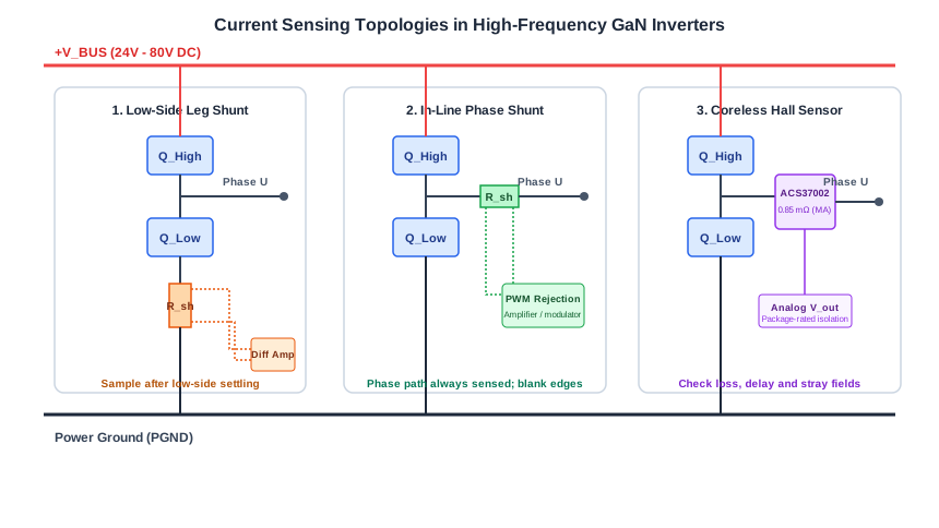
Current Sensing Architectures in High-Speed GaN Servo Drives: In-Line Phase Current vs Low-Side Shunts vs Coreless Magnetic Sensors
Compare current sensing in GaN servo drives: low-side shunts, in-line shunts and magnetic sensors. Use timing and thermal examples plus an RFQ checklist to select.
How to Specify 48V GaN Servo Drives for Low-Inductance Motors: Eliminating Chokes and Current Ripple
Specify 48V GaN servo drives for low-inductance robotics motors: current ripple limits, choke elimination, EMI risks, RFQ checks, and sourcing trade-offs.

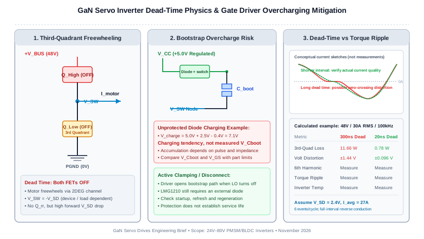
Dead-Time Optimization in High-Frequency GaN Servo Drives: Third-Quadrant Conduction Loss, Bootstrap Clamping, and Torque Ripple Mitigation
Dead-time optimization for GaN servo drives: estimate reverse-conduction loss, assess bootstrap protection, and compare supplier evidence with an RFQ checklist.