
Top-Side Cooling vs Bottom-Side Cooling in High-Power-Density GaN Servo Drives: Thermal Resistance Stackup, TIM Compression, and Robot Housing Integration
Compare top-side vs bottom-side cooling in GaN servo drives: evaluate thermal resistance stackup, TIM pressure, robot chassis heat transfer, and RFQ criteria.
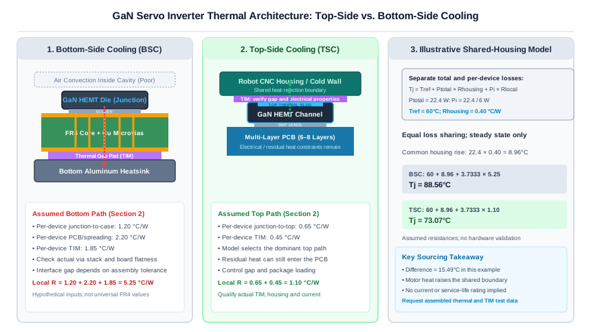
Top-side cooling vs bottom-side cooling in GaN servo drives is a choice about the complete heat path, assembly tolerances, and housing temperature. Top-side cooling can shorten the path from a power package to a robot housing. Bottom-side cooling can be competitive when the PCB, thermal vias, metal substrate, or copper inserts provide an effective path to the same housing. Neither architecture establishes a continuous-current rating by itself.
This comparison is for robotics hardware engineers, motion-control designers, and procurement teams integrating low-voltage drives into robot joints, cobot wrists, and AGV steering modules. In a sealed joint, motor losses can heat the housing that is supposed to cool the inverter. Package thermal resistance alone cannot answer whether the assembly will operate continuously.
Enhancement-mode GaN FETs have no intrinsic p-n body diode and therefore no associated body-diode reverse-recovery charge. They still have output-capacitance losses, reverse-conduction losses during dead time, and conduction losses that change with temperature. Small devices can concentrate those losses into a demanding local heat flux.
Key takeaways for sourcing and engineering teams:
- Compare complete paths: Request package, interface, PCB/spreading, and housing thermal data with their measurement boundaries.
- Separate local and shared losses: Each device's local thermal resistance carries its own dissipation; the common housing carries the sum. Multiplying total bridge loss by one device's junction-to-case resistance gives the wrong temperature.
- Treat TIM thickness as a design variable: A thin interface can reduce resistance, but must accommodate coplanarity and remain within the material's compression and electrical limits.
- Qualify the assembled joint: Housing temperature, adjacent motor heat, duty cycle, and sensor delay determine usable current. A component's headline current rating is insufficient.
- Check electrical coupling: Identify the thermal surface's electrical potential and evaluate insulation and displacement current for the exact package and interface.
Published and reviewed: November 8, 2026. Scope: Global engineering, sourcing, and architectural guide for low-voltage (24V–80V DC) GaN brushless servo drives in robotics, cobots, mobile automation (AGV/AMR), and compact actuator assemblies. Thermal models, tolerance calculations, and interface stackups are illustrative engineering frameworks to guide Request for Quote (RFQ) evaluations and hardware qualification.
For program-specific actuator sizing or custom mechanical enclosures, review our GaN low-voltage servo drive family or contact our team for an OEM custom engineering review.
1. The Physics of Heat Flux in Miniaturized GaN Inverters
A smaller semiconductor can dissipate fewer watts overall while producing more watts per unit area. Compare active die area, package contact area, and the much larger housing area separately: they are different boundaries, and heat must spread between them. Footprint area is not a measurement of active die area.
The following calculation uses six hypothetical discrete FETs. It is an arithmetic screening example, not a measured drive or a rating for a named semiconductor. For a real integrated half-bridge, use its multi-die thermal network and manufacturer guidance instead of treating two junctions as independent packages.
1.1 Quantifying Localized Heat Flux
Consider an illustrative 48V DC bus servo drive delivering 40A RMS (I_peak ≈ 56.6A) continuous phase current to a high-torque frameless joint motor at 100 kHz PWM.
For balanced sinusoidal phase currents, equal on-resistances, and synchronous conduction, assume a hot on-resistance of 3.5 mΩ per FET. Ignoring dead time and ripple, the bridge conduction estimate is independent of the arbitrary modulation-index value. The assumed losses are:
- Conduction losses:
P_cond ≈ 3 × I_RMS² × R_DS(on),hot = 3 × (40A)² × (0.0035 Ω) ≈ 16.8 W - Additional switching-related dissipation allocated to the six devices:
P_sw ≈ 5.6 W(assumed, not calculated from a device switching-energy curve) - Total Inverter Loss:
P_loss,total = 22.4 W
For this simplified equal-sharing model, each GaN HEMT dissipates:
P_loss,FET = 22.4W / 6 ≈ 3.73 Watts
Dividing the unrounded per-device power by an assumed active die area (A_die = 0.08 cm²) gives a local heat-flux estimate:
q'' = P_loss,FET / A_die = 3.73W / 0.08 cm² ≈ 46.6 W/cm²
This value describes the assumed die surface, not the whole PCB or housing. It does not predict junction temperature without the thermal path. Actual loss sharing depends on PWM, phase angle, dead time, and switching energy; stall can concentrate losses in fewer devices. Add PCB, shunt, controller, and gate-supply losses separately when estimating heat rejected by a complete drive. The assumed hot resistance must be checked again against the resulting junction temperature.
2. 1D Thermal Resistance Network: Mathematical Stackup
Use a steady-state thermal network for initial screening, then validate the actual assembly. For six devices sharing a housing, distinguish the local device path from the common housing path:
T_j,i = T_ref + P_total × R_housing + P_i × R_local,i
Here P_total is the heat entering the shared housing, P_i is the loss of device i, and R_local,i is its junction-to-housing path. An equivalent total-loss resistance can be formed only for the equal-sharing example: R_equiv = R_housing + R_local / 6. Do not insert a single-device thermal resistance into a total-bridge formula without this conversion.
2.1 The Critical Thermal Interfaces
- Junction to case: Use the thermal metric for the intended top or bottom surface, its stated test conditions, and its device/package power basis. A characterization parameter such as
ψ_JTis not interchangeable withR_θJC. - PCB and spreading: Bottom-side paths may include solder, vias, copper spreading, and board-to-baseplate contact. Determine whether a quoted measurement already includes any of these terms before adding them.
- Thermal interface: TIM resistance depends on compressed thickness, contact area, pressure, surface finish, and contact resistance. Bulk conductivity alone is insufficient.
- Housing to reference: This is the shared path. The reference must be defined: external air, a controlled cold plate, or another measured boundary. Internal cavity air and external ambient are not interchangeable.
2.2 Numerical Scenario: Equal Device Losses and a Shared Housing
Assume a fixed 60°C reference temperature, six equal device losses, and no additional motor or electronics heat entering the housing:
P_total = 22.4 W;P_i = 22.4 / 6 = 3.7333 W.R_housing = 0.40 °C/W, shared by all devices.- The resistances below are hypothetical inputs, not measured values for FR4, a particular via array, or a catalog drive. Their purpose is to show the accounting method.
Architecture 1: Bottom-Side Cooled (BSC) via PCB
- Assumed per-device junction-to-case resistance:
1.20 °C/W. - Assumed per-device PCB/spreading contribution:
2.20 °C/W. - Assumed per-device TIM contribution:
1.85 °C/W. - Local path:
R_local,BSC = 1.20 + 2.20 + 1.85 = 5.25 °C/W. - Junction estimate:
T_j,BSC = 60 + 22.4 × 0.40 + (22.4 / 6) × 5.25 = 88.56°C.
Architecture 2: Top-Side Cooled (TSC) to Housing
- Assumed per-device junction-to-top resistance:
0.65 °C/W. - No PCB term in this selected dominant top path; this does not mean zero heat physically enters the PCB.
- Assumed per-device TIM contribution:
0.45 °C/W. - Local path:
R_local,TSC = 0.65 + 0.45 = 1.10 °C/W. - Junction estimate:
T_j,TSC = 60 + 22.4 × 0.40 + (22.4 / 6) × 1.10 = 73.07°C.
The top path is 15.49°C cooler under these assumptions. Neither result proves continuous 40A capability, service life, or a protection trip time. The estimated junction temperatures differ from the 90°C condition used to select hot resistance, so a real loss/temperature calculation must iterate with device curves rather than treat these first-pass numbers as final.
If a motor also injects 30 W into the same modeled housing, the common temperature rise increases by 30 × 0.40 = 12°C for both architectures. A better package path cannot remove this shared boundary penalty. Unequal dissipation, mutual heating, parallel heat paths, and transient stall events require a coupled thermal model or measurements. Measure housing temperature at a defined point and use junction estimation appropriate to the device; do not infer junction temperature directly from a distant PCB sensor.
3. Bottom-Side Cooling (BSC): The FR4 Thermal Via Bottleneck & IMS Limits
Bottom-side cooling remains the default packaging method in the electronics industry because it relies on standard surface-mount (SMT) reflow assembly. The exposed thermal pad on the underside of each GaN package is soldered directly onto top-layer PCB copper.
3.1 The Physics of Thermal Microvia Arrays
FR4 dielectric material is a thermal insulator, with a low thermal conductivity of roughly k_FR4 ≈ 0.25 - 0.35 W/(m·K). By contrast, electroplated copper boasts k_Cu ≈ 385 W/(m·K).
To channel heat through the FR4 core to the bottom of the board, designers must drill dense arrays of thermal microvias directly beneath and around the transistor pads:
- Via Diameter: Typically 0.2 to 0.3 mm mechanical drill or 0.1 mm laser microvias.
- Plating Thickness: Standard 25 µm (1 mil) copper barrel plating.
- Fill Material: Epoxy-plugged and capped with copper (IPC-4761 Type VII) to prevent solder wicking away from the GaN pads during reflow.
A via-array resistance cannot be specified from via count alone. Record board thickness, finished hole diameter, copper plating or fill, pad area, plane connections, solder voiding, and the location of the cooled surface. Epoxy-filled, copper-capped vias are not equivalent to solid copper-filled vias. Blind microvias also do not create a complete through-board thermal path unless the stack connects to the receiving layers. Request the actual stack drawing and a board-level thermal result rather than assuming a universal resistance for FR4.
3.2 PCB Routing Layer Encumbrance
Beyond thermal resistance, bottom-side cooling can constrain routing in compact multi-axis drives:
- Inner Layer Piercing: Through-board via arrays occupy routing area; blind or buried structures affect only their connected layers.
- Current-Sense and Gate Loop Fragmentation: High-speed GaN gate loops require a short, controlled return path following the package-specific layout guidance. Vias on other electrical nets can require clearance openings in a reference plane; whether they disrupt a return path depends on the layout. Ground-connected vias can instead help connect ground planes.
- Power Bus Disruption: Phase-current sense traces (e.g., in-line shunts or low-side kelvin connections) must navigate around the thermal via fields, adding trace inductance and EMI susceptibility.
3.3 The Insulated Metal Substrate (IMS) Alternative
To eliminate FR4 thermal resistance, some drive designers build the power stage on an Insulated Metal Substrate (IMS)—an aluminum baseplate bonded to a thin copper foil via a thermally enhanced dielectric layer (k ≈ 1.5 - 4.0 W/(m·K)).
IMS can reduce the board contribution, but compare dielectric thickness, conductivity, effective area, and insulation requirements. It also creates integration trade-offs:
- Layer Count Limitation: Low-cost IMS boards are single-layer or two-layer only. Integrating the power bridge, gate drivers, and control electronics may require extra area or a separate control board.
- Daughtercard Complexity: Drive architectures must be split into a 2-layer IMS power card mated via board-to-board connectors or flex cables to an FR4 microcontroller/communication card. In high-vibration robotic arms and mobile AGV wheels, connector retention, vibration qualification, and service access need explicit review.
4. Top-Side Cooling (TSC): Direct-to-Chassis Heat Transfer & PCB Decoupling
Top-side cooling requires a package designed for a useful top thermal path. For example, the TI LMG2100R044 product page identifies exposed-top cooling and a bottom ground pad. That is a packaging example, not the device used in the hypothetical 40A calculation above. Higher-voltage GaN families are not automatically suitable substitutes in a 24V–80V drive.
Engineering Advantage of Top-Side Cooling:
A dominant top heat path can reduce the PCB thermal-routing burden. Electrical current, residual heat, return paths, and safety spacing still constrain every board layer. The architecture does not establish functional safety or a particular loop inductance.
4.1 Eliminating the Substrate Resistance
When the top path dominates, it can reduce dependence on board-through conduction:
- Obtain the actual junction-to-top metric from the device datasheet, including its measurement conditions; it is not a universal GaN property.
- Heat flows through a thin Thermal Interface Material (TIM) directly into the robot's CNC-machined aluminum housing, motor end-bell, or dedicated chassis cold plate.
- PCB thickness and copper weight still need electrical and thermal validation. Keep thermal vias when the manufacturer recommends them, even with a top heatsink.
4.2 Optimizing the High-Frequency Gate Loop
In a top-cooled layout, bottom terminals still provide electrical interconnections and can also conduct heat. Discrete devices may expose Gate, Kelvin Source, Power Source, and Drain terminals; integrated half-bridges have a different pinout.
- The gate driver IC can be positioned directly adjacent to the GaN pads, with the Kelvin source return routed on Layer 2 immediately below with a short return path consistent with the recommended layout.
- Minimize the commutation loop with closely coupled supply and return paths and local decoupling. Verify overshoot at the intended voltage, current, and slew rate rather than assigning an inductance from cooling architecture.
- For high-frequency motion control, explore our architectural analysis in Dead-Time Optimization in High-Frequency GaN Servo Drives and our guide on Current Sensing Architectures in High-Speed GaN Servo Drives.
5. The Mechanical Tolerance Trap: Component Coplanarity & Die-Cracking
Alongside its potential thermal advantage, top-side cooling introduces a critical mechanical failure mode that procurement teams and manufacturing engineers must audit: mechanical stress and die cracking during heatsink torquing.
5.1 The Coplanarity Challenge Across Multi-FET Bridges
A standard 3-phase GaN servo inverter incorporates six discrete HEMTs (or three half-bridge dual-die packages). When a flat metal heatsink or robot joint housing is bolted across these packages:
- Package Thickness Variations: Use the exact package drawing and lot tolerance; nominal height is insufficient for a clamp design.
- SMT Solder Stencil Variance: Measure post-reflow height variation from solder volume and assembly processing.
- PCB Bow and Twist: Specify local flatness over the contact footprint and include mounting distortion and housing flatness. A whole-board bow percentage does not define the local gap at every FET.
Illustrative worst-case coplanarity budget (assumed inputs):
Delta_z_max = Tol_package (±35µm) + Tol_solder (±25µm) + Tol_PCB_bow (±40µm) ≈ ±100µm
5.2 The Brittle Die Cracking Hazard
Unlike silicon power MOSFETs which are encapsulated in thick, compliant epoxy mold compounds (e.g. TO-220 or D2PAK), many high-density GaN devices are passivated wafer-level chip-scale packages (WLCSP) or ultra-thin QFNs with exposed silicon substrates. Silicon and gallium nitride are brittle crystalline materials.
A rigid heatsink and an insufficiently compliant pad can concentrate force on the tallest package, loading the die, package, or solder joints. Failure location and allowable force depend on the exact construction. Screw torque is not a direct measurement of package pressure: friction, stand-offs, fastener spacing, and plate stiffness change load distribution. Obtain mounting limits from the semiconductor supplier and validate the assembled clamp instead of using a generic fracture-stress number.
+-----------------------------------------------------------------------------------+
|               Rigid Heatsink Clamping on Uneven SMT Components (The Trap)         |
+-----------------------------------------------------------------------------------+
|  [ Rigid CNC Aluminum Heatsink / Robot Chassis ]                                  |
|  ====== [ Rigid High-Durometer TIM (Too Thin / Incompressible) ] ================= |
|                                                                                   |
|    +---------+            +---------+  <-- Tallest FET may take excess force    |
|    | GaN #1  |            | GaN #2  |      Risk: DIE / PACKAGE / SOLDER DAMAGE    |
|    | (Nom.)  |            | (+65µm) |                                             |
|  --+---------+------------+---------+-------------------------------------------  |
|  [ Multi-Layer FR4 PCB with Natural Reflow Bow ]                                  |
+-----------------------------------------------------------------------------------+
5.3 Engineering Solutions to Prevent Die Fracture
Three practical safeguards deserve review:
- Compliant TIM: Match the manufacturer's pressure-versus-deflection curve to the complete gap tolerance. A phase-change film is not automatically thick enough to absorb package-height differences before it softens.
- Travel limiters: Use stand-offs or shoulder features to define the minimum gap, while checking that the lowest package still contacts the TIM at the maximum gap.
- Controlled loading: Springs or washers can help maintain force over thermal cycling, but require a validated load range, plate stiffness, and package pressure limit.
For a pad with uncompressed thickness t0, compression is (t0 - gap) / t0. For example, a 0.50 mm pad spanning a 0.35–0.45 mm assembled gap sees 10%–30% compression. This arithmetic does not establish acceptability: compare both endpoints with the selected material's limits, thickness tolerance, creep, and the semiconductor's allowed load. Do not assume that a thin low-resistance film can absorb the illustrative ±100 µm height budget above. Tighter flatness, individual interface features, or a thicker interface may be necessary, with the thermal model updated accordingly.
6. Electrical Isolation & High-dv/dt Common-Mode Capacitive Coupling
In motor drive inverters, the thermal pad of a power semiconductor is rarely electrically neutral. Depending on the device package design:
- In some GaN packages, the top slug is internally connected to the Source terminal.
- In low-side switches, Source is connected to Power Ground (PGND).
- In high-side switches, Source is connected to the Switch Node (V_SW), which switches between the DC rails. Use measured edge rates and overshoot for the exact operating point; PWM frequency and edge slew rate are different quantities.
6.1 The Parasitic Capacitance Current Equation
When an electrically active thermal pad is pressed against an earth-grounded aluminum robot chassis, the Thermal Interface Material acts as the dielectric of a parallel-plate capacitor:
C_iso = (ε_0 × ε_r × A) / d
Where:
ε_0is the vacuum permittivity (8.854 × 10^-12 F/m).ε_ris the relative dielectric constant of the TIM (typically 3.5 to 6.0).Ais the thermal pad contact area across the three high-side FETs (A ≈ 0.3 cm²).dis the bond line thickness (BLT ≈ 75 µm).
Calculating the parasitic coupling capacitance:
C_iso ≈ (8.854e-12 × 4.5 × 3e-5 m²) / (75e-6 m) ≈ 15.9 pF
While 16 pF appears negligible at DC, GaN's extreme switching speed transforms this capacitance into a high-frequency current injector:
I_cm = C_iso × (dV/dt)
Under an assumed edge rate of 80 V/ns (80 × 10^9 V/s), for a device rated to support it:
I_cm = (15.9 × 10^-12 F) × (80 × 10^9 V/s) = 1.27 Amperes Peak
6.2 Sourcing & EMC Implications
The 1.27 A result is an idealized peak displacement-current estimate for the assumed combined area and synchronized transitions, not an RMS leakage current or an EMC test result. The three high-side nodes do not necessarily switch together; a real return network and its impedance determine pulse shape and current distribution. The 80 V/ns assumption is not a recommendation for the TI example: its datasheet, Section 5.2, specifies a lower recommended slew-rate limit.
Coupling can disturb encoder feedback or increase emissions, but this calculation alone does not prove bearing damage or an EMC failure. For feedback integration, see dual absolute encoder integration in GaN servo drives.
Procurement requirement: Identify whether each top surface is floating, source-connected, switch-node-connected, or internally insulated. Specify the required working voltage, insulation category, creepage, clearance, and test method for the actual application. Dielectric strength in kV/mm cannot be treated as the assembled interface withstand rating; compression, defects, aging, and edge paths matter. Lower capacitance may favor thicker or lower-permittivity material, while thermal performance may favor a thinner bond line. Resolve that trade-off with the selected material and system EMC plan.
7. Comprehensive Architectural Comparison Matrix
The following decision matrix evaluates the four thermal dissipation architectures relevant to low-voltage servo-drive integration.
Architecture alone does not determine current, inductance, capacitance, yield, or PCB cost. Use this matrix to request comparable evidence rather than assign unsupported numerical rankings.
| Selection question | Top-side to housing | Bottom-side through FR4 | Bottom-side through IMS | Embedded copper coin |
|---|---|---|---|---|
| Dominant heat path | Package top, TIM, housing | Package bottom, copper/vias, TIM, housing | Package, metal-substrate dielectric, baseplate | Package, coin, baseplate interface |
| Thermal evidence | Junction-to-top data and compressed TIM result | Actual via stack, spreading and interface result | Dielectric and interface impedance | Coin contact, spreading and interface result |
| Continuous current | Qualify in the actual housing and duty cycle | Same qualification required | Same qualification required | Same qualification required |
| Routing constraint | Can reduce thermal via burden; electrical constraints remain | Via clearances and return paths need review | Common low-cost stacks limit routing layers | Coin placement constrains routing and fabrication |
| Assembly control | Coplanarity, gap and load distribution | Solder quality, board flatness and baseplate contact | Dielectric integrity and baseplate flatness | Coin attachment, planarity and solder quality |
| Mechanical risk | Excess clamp load on packages or joints | Board bending and solder fatigue | Substrate stress and interconnect loading | Coin/laminate expansion and attachment stress |
| Electrical isolation | Check thermal-surface potential and TIM | Check copper/via net and baseplate interface | Check dielectric working voltage and edges | Check coin potential and isolation path |
| EMC evidence | Measure coupling area, capacitance and return paths | Same measurements; thick FR4 alone is no guarantee | Thin dielectric may increase coupling | Depends on coin area, potential and interface |
| Cost comparison | Include housing machining, TIM and clamp assembly | Include via fabrication and filling | Include substrate and control-board integration | Include special fabrication and yield allowance |
| Best-fit condition | Accessible housing above packages with controlled gap | Proven board path and convenient baseplate | Power/control partition is acceptable | Local heat spreading justifies special fabrication |
To review candidate drives matching these architectures, consult our catalog of robot joint servo drives and 100A high-power-density modules.
8. Thermal Interface Material (TIM) Selection Matrix for GaN Inverters
Selecting the correct TIM is just as critical as selecting the GaN semiconductor itself. A poor TIM choice can wipe out the thermal advantage of top-side cooling or destroy dies during mechanical assembly.
For a uniform layer, the bulk contribution is R_TIM,bulk = t / (k × A). With an assumed 0.10 mm compressed thickness, 5 W/(m·K) conductivity, and 10 mm² contact area, this is 2.0 °C/W before contact resistance. At 0.50 mm with the same area and conductivity it becomes 10.0 °C/W. Neither value is a product specification. The 0.45 °C/W interface assumed in Section 2 therefore needs its own verified area, bond line, spreading, and pressure; it cannot be inferred from a conductivity headline.
8.1 Phase Change Materials: Thin Interfaces with Contact Requirements
Phase-change materials can wet surface asperities after reaching their specified transition temperature. They suit small, controlled gaps, but initial contact, activation pressure, containment, and electrical properties remain product-specific. Request impedance versus pressure and thickness, initial assembly requirements, and thermal-cycle data. A film that performs well between flat test coupons may not bridge six packages with different heights. Do not assume a PCM is an electrical insulator or a substitute for a compliant gap pad.
8.2 Soft Elastomeric Gap Pads
Soft pads can bridge larger tolerances and simplify rework. Evaluate compression force, thickness tolerance, compression set, and performance after aging. A thicker pad can solve contact loss while increasing thermal resistance, so qualify the thermal and mechanical endpoints together. For optical encoders or other contamination-sensitive components, request material compatibility and outgassing evidence for the complete assembly. Silicone-free chemistry alone does not establish low outgassing, and silicone chemistry alone does not prove an optical failure.
8.3 Dispensable Gap Fillers
Dispensable fillers can accommodate irregular gaps and automated assembly, but require control of dispense volume, voids, cure conditions, slump, contamination, and rework. Low assembly force is not zero stress: cured modulus, thermal expansion, and adhesion can load packages during cycling. Include process inspection and end-of-line thermal checks in the supplier handoff. Compare total installed cost, including tooling, cycle time, scrap, and serviceability, rather than material conductivity alone.
9. Sourcing & RFQ Engineering Qualification Checklist
When issuing a Request for Quote (RFQ) or qualifying a GaN servo drive supplier for a mission-critical robotics joint, generic datasheet claims ("up to 50A peak") are insufficient.
Require candidate suppliers to document compliance against the following 8 engineering criteria:
- 1. Thermal-path evidence: Request exact semiconductor part numbers, top/bottom thermal metrics and their test conditions, and the assembled path to the housing. Do not add overlapping thermal metrics or compare values with different boundaries.
- 2. Continuous and peak duty envelope: Request current definitions (phase RMS, phase peak, or DC input), PWM frequency, bus voltage, motor duty, peak duration, cooldown, and thermal derating at defined housing and ambient temperatures.
- 3. Coplanarity and tolerance budget: Request post-reflow height measurements, housing flatness, board mounting distortion, minimum/maximum gap, and the proposed stand-off or travel-limiter drawing.
- 4. Package loading: Obtain allowed pressure, point-load restrictions, clamp geometry, assembly sequence, and a validated fastening process for the exact package. Agree a margin supported by these data rather than choosing a universal torque or pressure.
- 5. TIM identification and process: Record manufacturer, grade, uncompressed and compressed thickness, conductivity/impedance test conditions, compression range, aging behavior, and contamination compatibility. Define inspection and rework requirements.
- 6. Electrical and EMC interface: Identify every thermal surface's potential. Request assembled insulation evidence at specified working/test voltages and evaluate common-mode capacitance, switching edges, bonding, and encoder susceptibility.
- 7. Assembly durability: Agree thermal-cycle, vibration, humidity, and power-cycle conditions representative of the robot duty. Require test configuration, sample count, acceptance limits, and failure inspection; a named standard without a test profile is insufficient.
- 8. Protection and junction estimation: Identify sensor position, calibration, response time, junction-estimation method, and firmware trip/restart behavior. Validate short stall events and blocked cooling separately from steady-state testing.
Use this checklist during technical alignment meetings for our custom OEM motion control solutions and 10A micro joint servo drives.
10. Frequently Asked Questions
Why does a 98% efficient GaN servo drive still need a heatsink?
At 1,000 W input, 98% efficiency means 20 W loss; at 1,000 W output, loss is approximately 20.41 W. Both require a path to the environment. The efficiency figure does not identify which components dissipate the heat or their contact areas, and it cannot establish junction temperature without thermal boundary conditions.
Can we convert a bottom-side cooled drive by placing a gap pad over its FETs?
Only if the exact package supports a useful top heat path and the added mounting load is permitted. A molded top may have high resistance; exposed-die packages may behave differently. Consult the datasheet and mounting guidance rather than assuming every bottom-cooled device can or cannot benefit. Do not remove an existing bottom thermal path without validating the result.
How does thermal expansion mismatch affect top-side cooling?
The housing, PCB, packages, and TIM expand differently. A rigid clamp or adhesive can transmit shear into packages and solder joints. Compliant interfaces and controlled loading can reduce that stress, but need qualification across the actual temperature and vibration envelope. Nominal material expansion coefficients do not establish assembly fatigue life.
Does top-side cooling eliminate the need for heavy PCB copper?
No. The board still carries phase and bus current, and its own losses heat the joint. Select copper weight, plane geometry, vias, and connectors from temperature-rise and voltage-drop requirements. Top cooling can reduce one thermal constraint; it does not establish a universal copper thickness or eliminate manufacturer-recommended thermal vias.
How do we control common-mode noise into the robot chassis?
Identify active thermal surfaces, estimate interface capacitance and switching slew rate, and measure the assembled return paths. Balance TIM insulation, thickness, and permittivity against thermal needs. Bonding, filtering, and cable shielding must follow the complete system's grounding and safety design; a grounding strap alone does not guarantee EMC or protect encoder feedback.
What continuous current is possible in a 40 mm joint without a fan?
There is no general rating from diameter and cooling direction. Loss curves, PWM, housing temperature, motor heat, interface quality, and duty cycle all matter. As a bounded reference, TI's TIDA-010936 design reports up to 16 A RMS continuous without a heatsink at 25°C ambient and 40 kHz PWM. That reference does not rate a sealed 60°C joint or the hypothetical 40A example here. Require a supplier test matching your enclosure and operating point.
11. Conclusion & Next Steps for Robotics OEMs
In modern robotics engineering, mechanical packaging and thermal management are no longer secondary steps to be addressed after completing the electrical schematic. For compact robotic joints, dexterous humanoid limbs, and high-duty AGV traction wheels, the thermal architecture is the electrical architecture.
Choose top-side cooling when there is a short, accessible route to the housing and the production process can control package load and interface gap. Choose a bottom path when the board/baseplate assembly delivers adequate thermal performance with simpler integration. Improved vias, IMS, or copper coins may change that comparison substantially.
For either option, approve the complete housing, TIM, fastening method, loss envelope, and protection behavior together. The useful procurement outcome is a reproducible qualification configuration and a documented current-versus-temperature envelope, not a promise that one package orientation doubles torque.
Ready to optimize the thermal dissipation of your robotic joint actuators?
- Review our catalog of high-power-density GaN Low-Voltage Servo Drives and integrated EtherCAT 48V servo drive modules.
- For custom hollow-shaft geometries, multi-layer thermal interface modeling, or joint casing integration, engage our application engineering team for a Custom OEM Motion Control Solution.
- For mobile robot traction systems requiring high peak currents, explore our engineering solutions for AMR and mobile robot servo drives.
Sources & References
Sources checked on November 8, 2026. Manufacturer documentation supports the specific packaging and reference-design statements identified below. The worked losses, resistance stackups, compression budget, and capacitance calculation are explicitly hypothetical engineering examples; they are not first-party measurements, customer results, or supplier qualification records.
- Texas Instruments — LMG2100R044 product information. Identifies a top-cooled integrated half-bridge with a bottom ground pad. Its component rating is not an assembled servo-drive rating.
- Texas Instruments — LMG2100R044 datasheet, SNOSDF9B, Rev. B. Sections 5.2 and 5.4 define operating limits and thermal metrics; Sections 8.2 and 8.4 cover loss estimation, heat paths, and layout. These sections do not establish universal clamp-pressure or TIM specifications.
- Texas Instruments — TIDA-010936: 48V/16A three-phase GaN inverter reference design. Provides the bounded no-heatsink operating example cited in the FAQ. Its test conditions must accompany any comparison.
- Infineon Technologies — Gallium nitride product and technology overview. General GaN portfolio context only; this overview is not evidence for the numerical thermal scenarios, package isolation, or a particular low-voltage servo rating.
Author

More Posts
Regenerative Braking in Micro GaN Servo Drives: Sizing Brake Choppers, MLCC Bus Capacitance, and Shunt Resistors
Engineering and procurement guide for regenerative braking in low-voltage GaN servo drives: MLCC bus capacitor limits, brake chopper sizing, BMS disconnect risks, and RFQ checks.


Dual Absolute Encoder Integration in High-Speed GaN Servo Drives: BiSS-C & SSI Signal Integrity, Dual-Loop FOC Latency, and Mechanical Compliance
Dual absolute encoder integration in GaN servo drives: compare BiSS-C and SSI, budget feedback delay, and use an RFQ checklist to qualify your drive supplier.
Evaluating Monolithic 3-Phase GaN Servo Micromodules: 2026 Procurement & Engineering Guide
A 2026 engineering and procurement guide to monolithic 3-phase GaN servo micromodules, thermal limits, supplier risk, sourcing checklist, and fit for compact robotics.